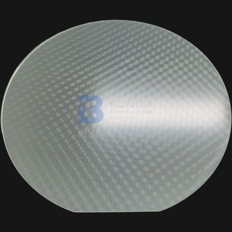
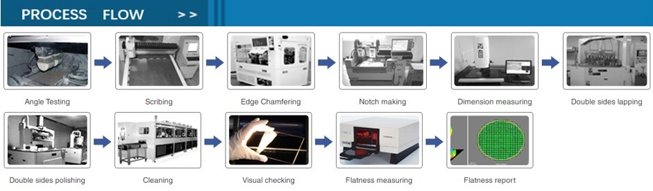
Product Description:
One of the key features of this product is its polished side Ra, which is less than 1.0nm or specific per requested, making it ideal for high-precision applications. The Fused Silica Wafer also has excellent transmission properties, allowing for ultraviolet and visible light to pass through with minimal absorption. This feature makes it an ideal choice for optical applications such as lenses, prisms, and windows.
The Fused Silica Wafer is available in different sizes, with a primary flat of 22mm, 32.5mm, 42.5mm, 57.5mm/notch, notch, notch, making it easy to choose the right size for your specific application. Additionally, the surface of the wafer can be either double-sided polished (DSP), single-sided polished (SSP), or double-sided lapped (DSL), depending on your needs.
In conclusion, the Fused Silica Wafer is a top-quality product that is highly suitable for various applications in the semiconductor industry. Its exceptional properties and different surface options make it a versatile option for your project needs. If you are looking for a reliable and high-quality Fused Silica Wafer, look no further than our product.
Features:
- Product Name: JGS1 JGS2 JGS3 Glass and Quartz wafer for Superior Optical Clarity Chemical Stability
- PLTV (<0.5um): ≥95% (5mm*5mm)
- Type: Fused Silica, Fused Quartz
- Thickness: 350um, 500um, 1000um
- TTV: <8µm, <10µm, <15µm, <20µm, <30µm, <30µm
Features of the Fused Silica Wafer product:
- Quartz Wafer
- SiO2 Wafer
- Silica Crystal Wafer
Technical Parameters:
| Parameter | Value |
| Diameter | 50.8mm, 76.2mm, 100mm, 150mm, 200mm |
| Transmission | Ultraviolet And Visible |
| Type | Fused Silica, Fused Quartz |
| Thickness | 350um, 500um, 1000um |
| TTV | <8µm, <10µm, <15µm, <20µm, <30µm, <30µm |
| Material | UV Fused Silica, Fused Quartz (JGS1, JGS2, JGS3) |
| PLTV(<0.5um) | ≥95%(5mm*5mm) |
| Warp | <30µm, <40µm, <50µm, <50µm, <60µm, <60µm |
| Application | Semiconductor, MEMS |
| Brand | JGS1 JGS2 JGS3 |
Applications:
The Fused Silica Wafer is suitable for a variety of applications. The wafer can be used in the semiconductor industry for the production of microchips. The wafer can also be used in the optics industry for the production of lenses, mirrors, and prisms. The wafer is also used in the solar industry for the production of solar cells. The Fused Silica Wafer is also suitable for research and development purposes.
The Fused Silica Wafer is available in different warp specifications, including <30µm, <40µm, <50µm, <50µm, <60µm, and <60µm. The wafer has excellent transmission properties in the ultraviolet and visible ranges. The wafer is available in both Fused Silica and Fused Quartz types. The wafer has a PLTV(<0.5um) of ≥95%(5mm*5mm), which ensures that the product has a high level of purity.
Overall, the BonTek Fused Silica Wafer is a high-quality product that is suitable for various applications. The product is made of high-purity materials and is certified by ISO:9001 and ISO:14001, ensuring that the product meets the highest quality standards. The product is available in different specifications and is suitable for the semiconductor, optics, solar, and research industries.
Support and Services:
Our Fused Silica Wafer product is backed by our team of experienced technical support professionals who are available to answer any questions or concerns you may have. We offer a range of services to help you get the most out of your product, including:
- Expert consultation to help you select the right product for your application
- Custom wafer fabrication services to meet your specific needs
- Technical support and troubleshooting assistance
- On-site training and support services
- Product repair and maintenance services
Our goal is to ensure that you are completely satisfied with your Fused Silica Wafer purchase and that it meets your expectations for quality and performance. Contact us today to learn more about our technical support and services.
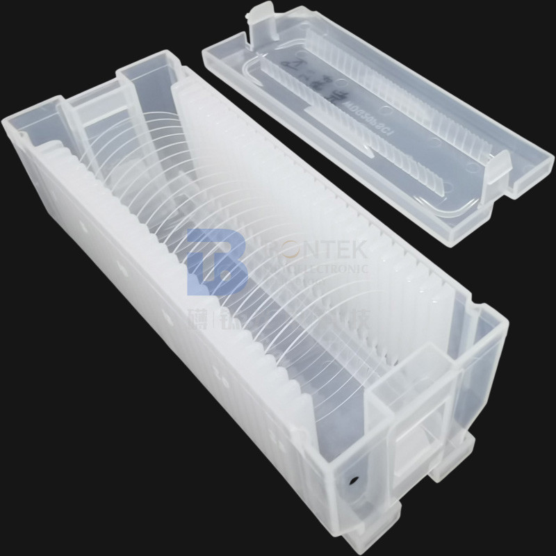
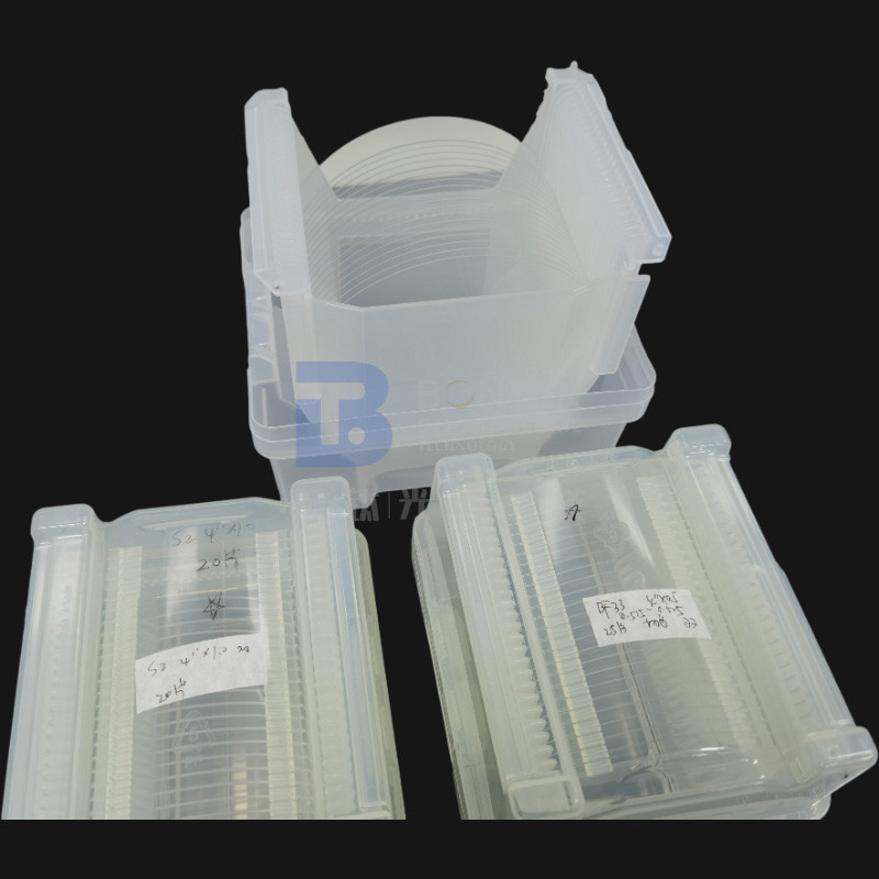
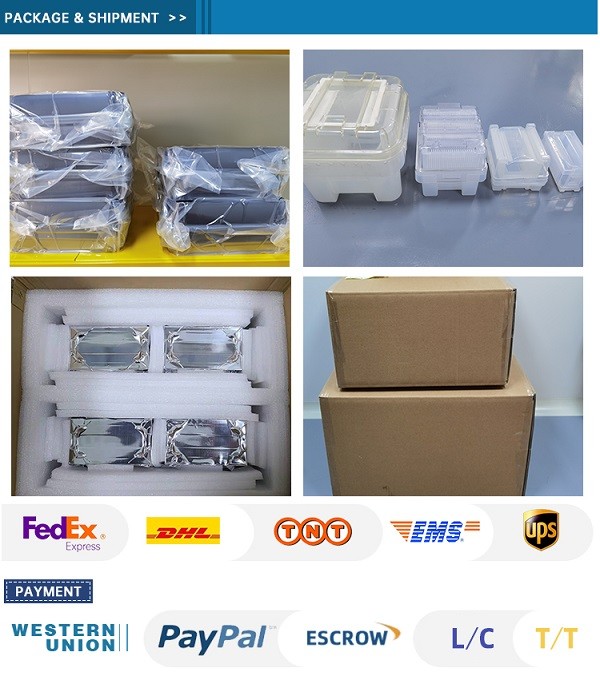
Packing and Shipping:
Product Packaging:
- The fused silica wafers are individually packed in cleanroom-grade polypropylene bags to prevent contamination.
- These bags are then placed in sturdy cardboard boxes with foam inserts for additional protection during shipping.
- The boxes are clearly labeled with the product name, size, and quantity.
Shipping:
- We offer worldwide shipping via trusted carriers, including FedEx, DHL, and UPS.
- All packages are insured to protect against damage or loss during transit.
- Customers will receive a tracking number once their package has been shipped.
- Shipping times may vary depending on the destination, but we strive to deliver products as quickly and efficiently as possible.
FAQ:
BonTek
2. What are the available models for the fused silica wafer?
Fused Silica, Fused Quartz
3. What certifications does the product have?
ISO:9001, ISO:14001
4. What is the minimum order quantity?
5 pcs
5. What are the payment terms for the product?
T/T
6. What is the supply ability of the product per month?
20000 pcs/Month
7. What is the delivery time for the product?
1-4 weeks
8. What is the packaging for the product?
Cassette/ Jar package, vaccum sealed
9. Is the price negotiable?
Yes, the price is negotiable.