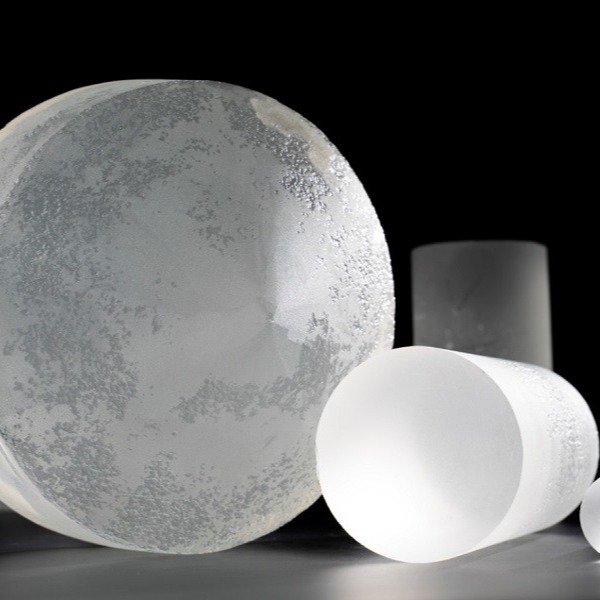
Pure Sapphire Crystal C-Plane Wafer for High-End Microelectronics and Power Devices
our premium Sapphire Wafers, the cornerstone of advanced technology and cutting-edge innovation. Renowned for their exceptional hardness, chemical stability, and optical transparency, Sapphire Wafers are the ideal choice for applications ranging from high-power optoelectronics and LED manufacturing to MEMS and biosensors.
Our Sapphire Wafers are meticulously crafted through advanced synthesis techniques and rigorous quality control, ensuring unparalleled crystal quality and surface smoothness. They offer superior thermal conductivity and mechanical strength, making them resilient to the rigorous demands of modern manufacturing processes.
Elevate your technology with our top-tier Sapphire Wafers. Their precision, durability, and versatility promise to deliver unparalleled performance across a wide range of applications. Discover the future of innovation with our premium Sapphire Wafers – order yours today and unlock the full potential of your cutting-edge devices and systems.
OPTICAL PROPERTIES
| Transmission | 0.17 to 5.5 um |
| Refractive Index | 1.75449 (o) 1.74663 (e) at 1.06 um |
| Reflection Loss | at 1.06 microns (2 surfaces) for o-ray - 11.7%; for e-ray - 14.2% |
| Absorption Index | 0.3 x 10⁻³ cm-1 at 2.4 um |
| dN/dT | 13.7 x 10⁻⁶ at 5.4 um |
| dn/dm = 0 | 1.5 um |
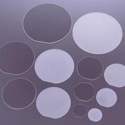
| Orientation | R-plane, C-plane, A-plane, M-plane or a specified orientation |
| Orientation Tolerance | ± 0.3° |
| Diameter | 2 inches, 3 inches, 4 inches, 6 inches, 8 inches or others |
| Diameter Tolerance | 0.1mm for 2 inches, 0.2mm for 3 inches, 0.3mm for 4 inches, 0.5mm for 6 inches |
| Thickness | 0.25mm, 0.33mm, 0.43mm, 0.65mm, 1mm or others; |
| Thickness Tolerance | 25μm |
| Primary Flat Length | 16.0±1.0mm for 2 inches, 22.0±1.0mm for 3 inches, 30.0±1.5mm for 4 inches, 47.5/50.0±2.0mm for 6 inches |
| Primary Flat Orientation | A-plane (1 1-2 0 ) ± 0.2°; C-plane (0 0-0 1 ) ± 0.2°, Projected C-Axis 45 +/- 2° |
| TTV | ≤10µm for 2 inches, ≤15µm for 3 inches, ≤20µm for 4 inches, ≤25µm for 6 inches |
| BOW | ≤10µm for 2 inches, ≤15µm for 3 inches, ≤20µm for 4 inches, ≤25µm for 6 inches |
| Front Surface | Epi-Polished (Ra< 0.3nm for C-plane, 0.5nm for other orientations) |
| Back Surface | Fine ground (Ra=0.6μm~1.4μm) or Epi-polished |
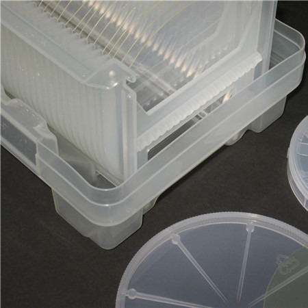
| Packaging | Packaged in a class 100 clean room environment |
Acceptance Check
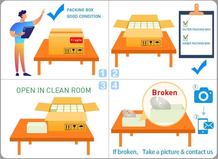
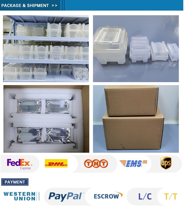
1. The product is fragile. We have adequately packed it and labeled it fragile. We deliver through excellent domestic and international express companies to ensure transportation quality.
2. After receiving the goods, please handle with care and check whether the outer carton is in good condition. Carefully open the outer carton and check whether the packing boxes are in alignment. Take a picture before you take them out.
3. Please open the vacuum package in a clean room when the products are to be applied.
4. If the products are found damaged during courier, please take a picture or record a video immediately. DO NOT take the damaged products out of the packaging box! Contact us immediately and we will solve the problem well.
Product Tags:

|
|
Pure Sapphire Crystal C-Plane Wafer for High-End Microelectronics and Power Devices Images
|